


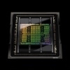
 As expected, NVIDIA presented a successor to an Ampere architecture called Hopper in the GTC 2022 Keynote. The GH100 GPU is the datacenter’s spin-off – similar to the previous architecture’s GA100 GPU. The GH100 GPU is manufactured at 4 nanometers in TSMC (N4) and NVIDIA limits the number of transistors to 80 billion. The predecessor had 54 billion transistors and was manufactured at 7 nanometers.
architecture hopper after Grace Hopper, an American computer scientist. NVIDIA remains true to its tradition of naming architectures after mathematicians and computer scientists. GH100 is the name of the GPU, H100 is the corresponding product.
The GH100 GPU is the first GPU to support PCI-Express 5.0 and uses six HBM3 chipsets with a memory bandwidth of 3TB/s and a capacity of 80GB. However, it appears that NVIDIA uses only five of the current six chipsets – just like the GA100 GPU. At the moment we cannot say why this is the case. However, yield in chip production should play a role here.
The GH100 GPU on the SMX should be allowed to draw 600W. This was roughly what was to be expected, after all, the predecessor had already reached 500W and there was a trend towards 500W and more for GPU accelerators for some time.

The central element of the GH100 GPU is certainly the computing units. NVIDIA is now releasing this Transformer Engine which is a type of tensioner core, which is now closely associated with the software. These modules mainly focus on 16 and 8-bit arithmetic operations, and the computing power of the H100 accelerator is 60 TFLOPS for double precision (FP64).
| H100 | A 100 | MI250X . Instinct | |
| Produce | 4 nm | 7 nm | 6 nm |
| number of transistors | 80 billion | 54 billion | 58 billion |
| FP64 processing power (TFLOPS) | 60 | 19,5 | 47,9 |
| FP32/TF32 processing power (TFLOPS) | 1.000 | 156 | 47,9 |
| FP16 processing power (TFLOPS) | 2.000 | 624 | 383 |
| FP8 processing power (TFLOPS) | 4.000 | – | – |
| storage | 80 GB HBM3 3 TB/sec |
80 GB HBM2 2 TB/sec |
128 GB HBM2E 3.2 TB/sec |
| PCIe | 5.0 | 4.0 | 4.0 |
| Link | NVLink 900 GB/sec |
NVLink 600 GB/sec |
INFINITI links 800 GB/sec |
| TDP | 600 watts | 500 watts | 560 watts |
First of all, it is certainly notable that NVIDIA is already using the TSMC N4 for the GH100 GPU, while the predecessor was still using the N7. AMD manufactures two Instinct MI250X chips at 6nm – also at TSMC. The complexity of the GH100 GPU becomes apparent when you look at the number of transistors. It should be 80 billion here. The GA100 GPU came in at 54 billion and the Instinct MI250X chipset came in at 58 billion.
As we explained earlier in the first section, the memory remains 80 GB. However, the change from HBM2 to HBM3 brings with it a significant increase in memory bandwidth. The 128GB Instinct MI250X is currently unbeatable in terms of capacity and bandwidth.
Comparing computing power is a bit tricky. NVIDIA specifies values for the shader output of the A100 accelerator as well as ideal use of tensor cores. We have included these extreme values in the table. As for the new H100 accelerator, we don’t yet know the exact architecture of the GPU and we’ve taken the values that NVIDIA gave us.

External communication is done on the one hand via PCIe 5.0, but in order to be able to exchange data models between several GPUs quickly enough, NVIDIA provides the fourth generation of NVLink. NVIDIA is talking here about the fact that an NVLink connection should achieve seven times the bandwidth of PCIe 5.0. According to NVIDIA, it’s 900GB/s per GH100 GPU. According to NVIDIA, the total external connection of the GH100 GPU is approximately 5 TB/s. The new NVLink also plays an important role with respect to the Grace processor. But more on that in a separate post.
Transformer drive and fourth generation of core tensioner
For the hopper structure, the focus is again on maximum flexibility. The H100 GPU accelerator should be able to perform high-precision scientific calculations with dual precision (FP64) and those for AI applications (INT8, FP8, and FP16) – with the best possible use of available resources.
On the other hand, NVIDIA offers 4th generation Tensor cores with the Hopper architecture and combines them with a program or implementation layer called Transformer Engine.
The hopper structure tensor cores can run mixed FP8 or FP16. For FP8, the transfer rate is 2 times higher than for FP16. NVIDIA-trained inferences determine whether computations are performed in FP8 or FP16. TensorFloat32 (TF32) remains the standard format in TensorFlow and PyTorch, but these calculations are broken down into FP8 and FP16 by the Transformer Engine in order to use devices in the form of Tensor Cores as optimally as possible.
What has been described so far relates to training AI models. INT8 computations are still important for inference. It can also be optimized for hopper architecture and then computed, so that H100 accelerators are also significantly faster compared to their predecessors.
NVLink Switching System
Not only is NVLink used to connect eight GH100 GPUs in the DGX-H100 system, but it can now be expanded to full racks with the NVLink switching system. Up to 256 H100 GPUs can be integrated via NVLink.


The total bandwidth of the NVLink switching system is 70.4 TB/s. Managing such a network also requires its own computing power, which according to NVIDIA should be 192 TFLOPS. For comparison: The new Spectrum-4 Ethernet switch achieves 50.2 Tb/s (6,275 Tb/s).
In addition to being integrated into the GH100 GPU, the Grace Hopper, and the Grace CPU Superchip, NVLink is also opening up as a standard that other chip makers can adopt to interact with NVIDIA devices they connect directly to.

NVIDIA expects the H100 GPU accelerator to be nine times faster than its predecessor. This is definitely also related to the application in question. The main thing is to reduce the times of individual training sessions.
The H100 GPU will be available on both an SMX card and a PCI Express card. Additionally, NVIDIA is packing the H100 GPU with ConnectX-7 on the PCB. In edge computing, the advantages of fast communication and processing must be exploited.
Starting in the third quarter, NVIDIA plans to introduce its first H100 GPUs. It is said that production has already started. NVIDIA will build its own supercomputer based on the H100 GPU accelerator. This will consist of 576 DGX H100 systems, each with eight H100 systems.

“Problem solver. Proud twitter specialist. Travel aficionado. Introvert. Coffee trailblazer. Professional zombie ninja. Extreme gamer.”
More Stories
With a surprise in the case: a strange cell phone from Nokia was introduced
PlayStation Stars: what it is, how it works and what it offers to its users | Sony | video games | tdex | revtli | the answers
t3n – Digital Pioneers | digital business magazine